Arima PV&O has been focusing on development of single- and multi-junction III-V solar cells since year 2007.
Our goal is to become a major supplier providing high C/P value and reliable solar cells for terrestrial, space and consumer applications.
Maximum triple junction (TJ) cell efficiency under concentrated suns reaches 42%.
Average TJ cell efficiency in production exceeds 39.5%.
-
Single Junction GaAs Solar Cell

1. Front and back contacts are weldable or solderable
Learn more
2. Cells are fully tested under AM1.5D illumination -
Triple Junction Solar Cell (InGaP/InGaAs/Ge)
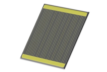
1. Front and back contacts are weldable or solderable
Learn more
2. Cells are fully tested under concentrated illumination -
Space solar cell
1. Triple junction solar cell (InGaP/InGaAs/Ge)
Learn more
2. Front and back contacts are weldable or solderable.
3. Cells are 100% tested under AM0 illumination -
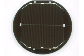
Triple Junction Concentrator Solar Cell Epiwafer
1. Growth by MOCVD tech.
Learn more
2. High efficiency, triple junction solar cell, with n-on-p polarity on Ge substrate -
Arima HCPV System Installations
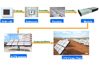
1. Has been certified by International
Learn more
Electrotechnical Commission (IEC)
2. Has constructed numerous HCPV facilities -
Photolithography process area
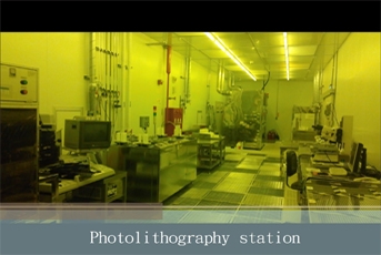
Class 1,000 yellow room equipped with photo-resist spray coater, mask aligner, photo-developer, oven, spin dryer and hot N2 dryer.
Learn more
Epiwafer size processed is from 2- to 6-inch . -
Wet chemical station area
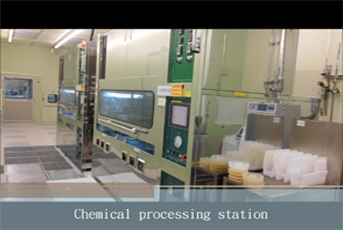
Equipment including acid wet bench, alkaline wet bench, organic clean wet bench and photo-resist strip bench.
Learn more -
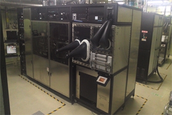
Thin metallization film area
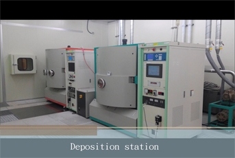
Equipment including two E-beam evaporators for contact metallization and a rapid thermal anneal (RTA) set-up for contact annealing.
Learn more
Thickness uniformity is well controlled.
Evaporation angle is also well controlled. Front metal gridline profile is >80 degrees. -
Saw dicing area
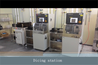
High-speed rotated diamond dicing equipments are used for saw dicing.
Learn more
Dicing width and depth are well controlled.
Chipping and breakage have been reduced to very minimal.
Heat generated from dicing is reduced by in-situ water cooling system. -
Cell testing area
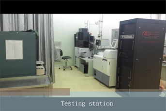
Solar simulator is utilized for measuring optical-electrical transfer efficiency on wafer, chip and sub-mount level.
Learn more
The concentration ratio of simulator can be adjusted from 1- to 2,000-suns.
Quantum efficiency (QE) measurement set-up is used to measure cell QE from 300 nm to 1800 nm spectral wavelengths. -
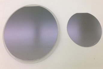
MOCVD epitaxial growth area
Arima PV&O utilizes MOCVD technology to grow epitaxial wafers.
Learn more
Standard wafer size is 4-inch. Other wafer sizes including 2 inch, 3 inch and 6 inch are also available.
Arima PV&O’s standard epitaxial products are
GaInP/InGaAs/Ge triple junction solar epi wafers,
GaInP/GaAs dual junction solar epi wafers and
GaAs single junction solar epi wafers.
Other customized epi wafer is also available upon request.