MOCVD epitaxial growth area
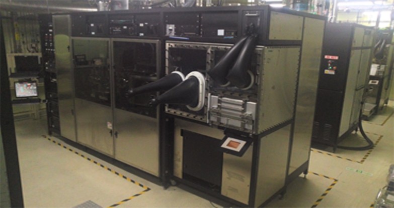
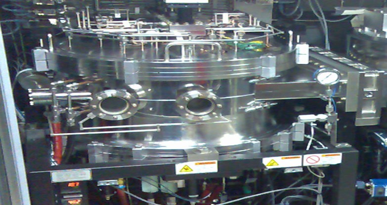
Arima PV&O utilizes MOCVD technology to grow epitaxial wafers.
Standard wafer size is 4-inch. Other wafer sizes including 2 inch, 3 inch and 6 inch are also available.
Arima PV&O’s standard epitaxial products are
-GaInP/InGaAs/Ge triple junction solar epi wafers,
-GaInP/GaAs dual junction solar epi wafers and
-GaAs single junction solar epi wafers.
Other customized epi wafer is also available upon request.
- Introduction
MOCVD, Metal-organic Chemical Vapor Deposition, is to grow epitaxial thin film on the substrate. Other names used including
(1) MOVPE (Metal-Organic Vapor-Phase Epitaxy),
(2) OMVPE (Organometallic Vapor-Phase Epitaxy) and
(3) OMCVD (Organometallic Chemical Vapor Deposition).
The first two letters "MO" or "OM“ means the reagent source (precursor) is either the “metal-organic" or the “organnometallic compounds”.
MOCVD – technical advantages
(1) can grow a variety of compound semiconductors;
(2) can grow high-quality materials;
(3) can grow thin epitaxial layers;
(4) can grow hetero-structures;
(5) the grown thin film with good uniformity on large area,
(6) Best technology for high volume production.