Home / Business Divisions / Solar Energy / Solar Cell Business Unit / Triple Junction Concentrator Solar Cell Epiwafer
Triple Junction Concentrator Solar Cell Epiwafer
1. Growth by MOCVD tech.
2. High efficiency, triple junction solar cell, with n-on-p polarity on Ge substrate
- Introduction
- Specification
- Characteristic
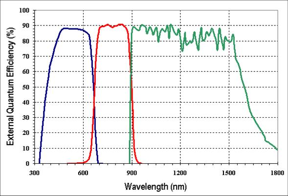
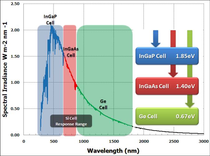
1. InGaP/InGaAs/Ge Triple Junction
2. For high concentrated (HCPV) application
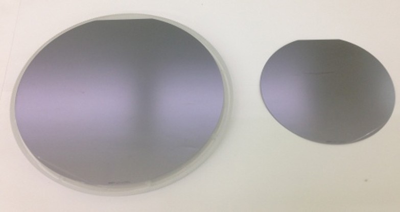
3. 4 or 6 inch epiwafer
2. For high concentrated (HCPV) application
3. 4 or 6 inch epiwafer
| Item |
Measurement
|
Specification | Notes |
| Visual Inspection | Wafer surface scratches edge chippings particles/defects | No visual scratch and chipping For large size particle and defect by visual inspection: a) size ≦ 2 mm,≦8,and b) 2-3 mm, ≦ 5,and c) 3-5mm,≦ 2 |
Visual scratch and chipping mean length or size > 0.25 mm |
| Epi layer structure | (1) Layer thickness (2) Carrier concentration |
(1) Deviation ≦ 10% (2) Deviation ≦ 20% |
(1) Total epi-layer thickness 7 um (2) Contact layer 0.5 um (3) Diffusion thickness of autodopants into Ge substrate back side is 1.5 um (4) Contact layer concentration >1 E19 cm-3 |
| Wafer Thickness | Thickness | (1) 185 ± 20 um (range) -within wafer | |
| Electrical | IV characteristics | (1) Jsc: 13.5 mA/cm2 (minimum: 13 mA/cm2) (2) Voc : 2.53 V (minimum: 2.48 V) Efficiency > 27% |
Quick lot process with AR-coating material and chip active area is 0.3003 cm2 Typical characterisrics at one sin, AM 1.5G,25℃ |